Archive

Electronics

Many have shared their experiences replacing the drained real-time clock (RTC) batteries on their GBA Pokémon games. Few have referenced Natalie Imbruglia in the process.

I knocked this video out for the sake of knocking a video out; you’ll observe unscriptedness, camera-quality audio, lots of text added in post, jump cuts, vocalized pauses, heavy breathing and an obnoxious nasalness in the voice (the latter two because I’m a little under the weather). Even the tiny theme song is a bit on the disappointing side. But, as they say, you can’t optimize code that doesn’t exist. After some scrutiny of this entry, maybe next time will be better.

I’ve designed at least three or four different multi-74HC595+NMOS boards[1] over the past couple of years, but I believe this most recent one is the first one that ever worked on the first try.

Before I get to any specifics about that, here is a bit about how it was soldered.

Preflow

My technique has advanced since when I first experimented with plain solder reflow so many moons ago. I’ve developed this into a methodology I’m starting to refer to as “preflow” due to its relationship with reflow soldering. It’s nothing new and I even got the idea from multiple other sources, but I’d like to document the specific flourishes I’ve needed to apply to make it work for me.

We like reflow soldering because it’s an effective way to get SMT[2] parts attached correctly to a board, enabling us to perform the most delicate and error-prone task of initially positioning parts without heat (important to me because I have shaky hands and need the extra time).

Typically, solder paste and a solder paste stencil are used in the reflow process.

  • Solder paste allows the placement of SMT components without the immediate use of heat.
  • Solder paste is somewhat viscous and helps prevent the placed components from accidentally moving or becoming misaligned before the board is reflowed.
  • A stencil precisely applies a metered amount of solder paste, which avoids excess solder that might cause bridging or imbalanced solder that might cause a component not to mount flush with the board.
  • A stencil applies solder for the entire board, or even a whole panel of boards, in a single, very short pass, saving large amounts of time for production at any non-trivial volume.

But, as a hobbyist or for R&D purposes, perhaps we don’t care for solder paste or stencils.

  • To use solder paste as recommended, we need to buy either a rather expensive small quantity or a larger quantity at a lower unit price. It does expire, so assuming we’re not producing in volume, the latter is no more economical. (Expired paste can reportedly be refreshed with the addition of some flux, but the result is a bit muddy and uneven compared to the fresh stuff.)
  • Any significant leftover quantity must be refrigerated for longevity. This requires either a separate refrigerator or the willingness to keep a somewhat toxic, lead-based compound in proximity with things that need to remain edible.
  • We’re not willing to waste money proactively ordering the stencil for a board design that we haven’t yet tested. (But solder paste without a stencil is a sticky, unworkable mess.)

This technique fills the roles ordinarily filled by solder paste and stencils with ordinary solder and paste flux. The main idea is to ensure that every pad has an appropriate amount of solder before placing the components.

  • A soldering iron is used to apply solder to all pads. This puts solder everywhere it needs to go, like a stencil would. This part can be done quickly and imprecisely; the point is to ensure that no pad has too little solder.
  • Manual soldering/desoldering techniques are used to remove excess solder and clear any bridging of adjacent pads.
  • The board is “preflowed”: Flux is applied and the board is reflowed without any components in order to cause the solder to go, in so many words, where it goes when the board is reflowed. This step may seem superfluous, but it’s proven to be important. The preflow clears irregularities introduced by the manual process by redistributing and recentering the solder on the pads. This creates a sort of “print preview”, revealing any edits you might need to make to prevent bridging[3], dry joints [4], tombstoning [5], and so forth.
  • If necessary, use manual soldering/desoldering to edit the solder, then repeat the preflow step.
  • The solder now being in all of the right places, flux all the pads on board again using paste flux. The flux will be necessary for the reflow (as it is with solder paste, which has the flux already mixed in) and has a thick enough consistency to keep components from moving too much when placed.
  • Place the components and reflow as normal.

The big con to doing it this way is the amount of time it takes; compared to paste and stencils it just does not scale at all. If I had to produce, say, 10 of the same well-tested module at a time it might be worth my while to gear up. But in my world, it’s usually new and untested design that I’m receiving in threes from Oshpark, and even having a stencil made doesn’t make any sense.

Ingredients

To do this stuff, you’ll need:

  • A decent soldering iron. Mine is a Hakko FX-888. A cheaper one will probably do here, but a good iron is good for sanity.
  • Copper cleaning wire for your iron (that is, the thing that looks like a copper scouring pad) or something else that will quickly and easily remove the excess solder from the tip of the iron.
  • Accessories for desoldering by hand. At least desoldering braid/wick is pretty necessary for the subtler editing steps. A vacuum pump tool is useful for larger bits of excess solder.
  • Ordinary flux-core Sn/Pb solder wire. (Lead-free might work, but I can’t vouch.)
  • Reflow oven or other apparatus for reflowing a whole board. I use a reflow skillet, just some Rival electric skillet, which I nominally set to 375°F (a little over 190°C).
  • No-clean paste flux, for fluxing the pads just before placement. MG Chemicals 8341 is what’s on hand here. It must be paste; liquid flux won’t do here.
  • A well-made PCB to receive the circuit.
    • The board must include any solder mask that may be necessary. (Generally true for any reflow.)
      • The current success follows on previous designs that experienced issues due to the solder mask clearance of a tiny SC-70 part not being tight enough to prevent bridging. This may be less of a concern if you aren’t designing your own footprints for parts like this.
      • If you attempt to make homemade solder mask, make sure no part of it is flux-soluble. The previous article detailed how bad of an idea it is to try to use marker ink as solder resist. In a more recent experiment, stripboard with polyimide tape (“Kapton”) turned out to be a bad choice; the flux mixed with the tape’s adhesive and turned the board into a viscous piece of slop—and the result wasn’t even effective, leaving over half the board needing rework by hand.
    • The pads must be the correct shape and size for the components. (Also generally true for any reflow.)
      • This has also been a point of trouble for my homemade boards. Reflow soldering done on an appropriately made board helps components drift into position due to some surface-tension-related phenomena, but trying to get a 0603 resistor to stick correctly to a place I hastily scratched out for it from some stripboard didn’t go smoothly.
  • Optionally:
    • A hot air rework tool. This doesn’t replace your reflow oven/device for the ultimate reflowing of the board itself—it produces an air current, which isn’t what you want after ten or twenty minutes of carefully placing components—but works nicely for the preflow phase. Mine is something I found on either Amazon or Aliexpress using the search term “858D”. One can still be had around $30, and it’s a purchase I don’t regret. It is always set to 350°C; there never seems to be any reason to change it.
    • No-clean liquid flux. This doesn’t replace the paste flux for when you place the components, but for every other phase it’s a bit less messy (and just nice to have around for general-purpose soldering).
    • Spray flux remover with a brush-tipped nozzle. All of the flux used here will leave the board tacky. This helps fix that. Isopropanol and ESD-safe cleaning brushes can also be used but tend to be a bit more work.
    • A microscope or eye loupe for visual inspection. I picked up a product advertised as a 60X currency-detecting pocket microscope (it has white LEDs for plain illumination and a blacklight LED for verifying big bills) from Aliexpress for under $2. Very cheap, gets the job done, must recommend.

Editing

So far, editing the solder on the boards has involved clearing up these issues:

  • Solder going where it shouldn’t or not going where it should. If the solder refuses to move in a way that is at all helpful, apply flux to the solder and pads and try again. (This turns out to be great advice for soldering in general. Flux is way more important than you might realize. Soldering without flux is masochism. Flux is the secret sauce to this whole activity.)
  • Too little solder. A flat pad won’t properly attach to a component lead. Just add more solder.
  • Too much solder. A pad with enough solder on it has a subtle, shiny dome. It shouldn’t look stuffed like a pillow. In general, if you brush off the iron tip, touch it to a pad, and then drag it away from the pad, it shouldn’t take (much) solder with it. Incidentally, this is also an okay way to correct the problem; take excess solder away with the iron tip, brush off the tip, and repeat.
  • Way too much solder. If there’s anything on the board resembling a drop of solder, get rid of it. I use the vacuum tool for this one.
    • That said, avoid using the vacuum tool for more delicate work. I’ve had the nozzle of a vacuum tool bend or scratch up pads and traces.
  • Bridging between IC pads. If adjacent pads are sticking together, brush off the tip of the iron and then run it along the length of the pads in sort of a combing motion. If the iron isn’t picking up the excess solder even after brushing off the tip, there might be too much solder. The desoldering braid is useful here.
  • Imbalanced pads. All pads for the same component should have the same amount of solder. If any pads have visibly different amounts of solder than the others, when reflowed they may fail to sit flush with the board or make adequate connections with all pins. Adjacent pads can be balanced somewhat by passing the iron across them repeatedly, which may take excess solder from one pad and deposit it on another. If the balanced pads ultimately contain too little or too much solder, see the previous advice.

The mk 2, v1.10.1

Last August, I designed the most recent iteration of the board, but hadn’t assembled a copy until yesterday. (This module was to be part of a scoreboard feature for my family Fall Party, which for the past two years has featured game shows on stage, but I had to abandon the scoreboards and move on to the buzzers and other features closer to completion.)

Various problems had plagued the boards previously, and ultimately each byte would have a couple of non-functioning bits. The footprint I’d used for the SC-70 transistor packages had the solder mask set so loose that adjacent traces were exposed which tended to bridge easily. One pass had the transistor packages themselves adjacent rather than staggered, which caused the surface tension effects to draw one of them in between where two of them were supposed to go. Naturally, a well-designed board is important for reflow soldering, and this edition had removed all of the glaring errors.

Preworked.

The prework procedure described above resulted in a nicely pre-soldered board. The solder pads are all shiny and even-looking.

Pasted.
(Top: A syringe of paste flux. Left: A homemade stripboard masked with polyimide tape to demonstrate what not to do.)

The next step was to coat the exposed solder with paste flux in order to hold things in place and make the solder act in the way solder must.

Positioned.

Components are carefully put into place. Note the decoupling capacitor beside each IC being slightly off its mark. The two-contact components don’t sit quite stably on the domed tops of the solder pads. This isn’t a problem, though, because the surface tension effects of the solder will gently pull the component into place. This is actually kind of useful, as it provides a visual indicator that the reflow skillet has heated up enough to melt solder.

Piping.

The entire thing goes into the skillet to attach everything. If you look closely, you can see a bit of trouble.

In the process of reflowing, one of the ICs and two of the transistor packages drifted slightly askew. Still, this sort of thing happens from time to time during reflow soldering, and out of 18 components, 3 isn’t that bad. I wonder if perhaps using less paste flux, or brushing it down to an even layer, would help prevent parts from floating off like this.

Proper.

With a little more flux, the hot air tool, and a minute or two of light nudging (it took surprisingly little time), the wayward components were restored to their proper places. Through-hole parts were added, a bit of Flux-Off removed the excess glop, and the device was ready. After attaching it to an Arduino and firing up a test sketch, much to my pleasant surprise—and I do mean surprise—it turns out all 24 bits are firing as they should. No going back with the continuity tester to find a mistake or anything. A true wonder!

  1. [1]74HC595, as you may or may not know, is a parallel-out shift register, which can be used to switch a large number of outputs over a small number of wires. Adding N-channel MOSFETs (sometimes known as “NMOS”) to the outputs allows them to drive higher current outputs.
  2. [2]surface-mount technology
  3. [3]Connection between adjacent pads or traces by a single blob, usually unintentional
  4. [4]Insufficient solder on a joint to make an effective connection
  5. [5]The habit of a usually 2-terminal component to stand up on one end after soldering, often caused by the effects of having a larger solder blob on one pad than the other

As happens on a fairly regular basis these days, the two- to six-week shipping wait came to an end last night for another so-cheap-as-to-be-questionable eBay electronics purchase from China or Hong Kong. This time, it was an item called “New Mini Mirror Clip Mp3 Sport Music With TF-Card[1] Slot Up To 8GB”. I purchased two of these for $1.45 each, shipping included, with the intention of cracking them open and controlling them using a microcontroller[2], but also with the knowledge that even the non-MP3 parts, including a 3.5mm stereo jack, a USB mini-B jack, a microSD slot, a little rechargeable battery, and maybe some other goodies, would justify the already trifling cost as scrap.

The Player Itself

Backed by a $5 memory card and a USB cable from a far more expensive Sony music player, this tiny device somehow fails to be irrelevant.

Before I went to work on taking it apart, I set about making sure the thing actually worked. Because I didn’t have a card adapter handy, I used the USB interface on the device itself. It’s not fast by any stretch of the imagination—I think it actually uses USB 1.1 (and, after having looked at the guts, I’m guessing the low-speed SPI interface on the card). I put on files in four formats—MP3, WAV, Ogg, and FLAC—in order to determine what it would actually play.

The results are these: Only the MP3 file played. After changing the extensions on the other files to .mp3, the WAV file also played, but the others were still skipped. And while the output of the audio content itself was adequate, there was substantial background noise carried over from the rest of the circuit. For under $8 including the shipping and the memory card, we’re not expecting a hi-fi or even an iPod shuffle—but this is a reminder that we’re working with something suitable for little more than a toy. And that’s okay, because the less shady version of an MCU-controlled MP3 decoder will set you back $40 from a finer (and more legitimate-feeling) retailer.

MP3 player with front face slightly separated

The device comes apart with a light touch.

No screws were visible on the device, so I set about coercing it apart by running my thumbnail down a seam on the face. As you can see, it was more than cooperative. (That said, I think it would take a non-trivial impact for it to come apart on its own.)

MP3 player with mirror face detached

Pink.

The mirror face is actually kind of like a sticker with a backing having roughly the malleability of thin sheet aluminum. It was stuck by a tacky adhesive to the back of the face, which was a slightly thicker piece of pink plastic.

MP3 player with face removed and tactile domes exposed

Clickity.

The rest of the face comes off easily, revealing the PCB with five tactile domes (the kind that deform under your finger and make an obvious click when depressed) taped in place.

MP3 player with tactile domes partly removed

The domes and contacts.

MP3 player with tactile domes removed

Bull’s eye.

Under each dome are concentric outer and inner contacts on the PCB; pressing the dome connects the center to the surrounding ring, registering a button press.

Freeing the PCB from the case was slightly more than my thumbnail could muster, so I used a prong from the plug end of a phone charger I had handy. As before, it was only lightly stuck into place and required only trivial force to remove.

MP3 player full PCB and battery

The guts.

The internals of this thing, at least from what I can see without desoldering anything, are amazingly simple. Other than a number of discretes countable on one or two hands, you have the battery, the microSD slot, the stereo jack, the USB jack, a very small switch (I think SPDT), and the main event—an SOIC-16 chip running the whole show.

Detail of MP3 player PCB

I don’t know who this “JL” guy is.

The latter is marked with a logo that looks like somewhere between “JL” and “π”, followed by the cryptic legend “AB1426CF3Y13.1-83En” for which Google proves useless to make any connection.

Several of the pins on the microSD card are kept intentionally disconnected (there even appears to be a bit of silkscreen to prevent their accidental connection), which is why I think the SPI mode (which uses fewer pins than the full-speed modes) is in use.

Anyway, the whole thing is actually surprisingly simple connection-wise (a good deal less complex than the player in original Instructable). I kind of wonder if I could perhaps get the whole thing desoldered, reverse-engineer a schematic, and put it back together in a way that would have fewer noise issues.

Fun.

  1. [1]TransFlash, or “TF”, is an outdated name for microSD. Given that microSD is far more recognizable, and that an 4GB or 8GB card is not even plain microSD but microSDHC, I have no idea why they’d call it by this name.
  2. [2]in a similar fashion to this Instructable which uses a somewhat more expensive but mostly identical player

A simple one-directional level shifter is easy to build out of an NPN transistor and two resistors in the common-emitter topology, if the application doesn’t need to sink as well as it sources—that is, if a significant output impedance is acceptable when the output is high. If low impedance is needed for high output, an additional PNP transistor and two resistors[1] can be added, again in common-emitter topology, to re-invert the signal, but then the output low has the impedance instead.

To both source and sink with comparably low impedances, the obvious solution, if you’re properly equipped, is probably CMOS: Two complementary MOSFETs configured to pull the output either up or down, with similarly low impedance either way—or, more likely, a CMOS logic IC that does the same thing, but in a more compact fashion.

Still, there are some possible issues:

  • If you don’t keep a stock of (fairly well matched) N-channel and P-channel FETs around, you can’t really build a CMOS inverter out of them.
  • If all you have are 74HC-series ICs, the output voltage must be from 2V to 6V. If your output voltage is, say, 13V, this is a no-go.[2].
  • If the input high voltage is too much lower than the output voltage, a logic high may not register properly. A preliminary low-to-high shifter (such as the single-sided NPN thing from before, 3 parts) would be needed for each input.
  • If the input high voltage is too much higher than the output voltage, a logic high may do some damage to the IC. A preliminary high-to-low shifter (such as a resistive divider, 2 parts) would be needed for each input.

Incidentally, constructing a CMOS-like complementary output using discrete bipolar transistors is not advisable;  even short input transitions can cause high and low transistors to be on simultaneously for a non-trivial amount of time, a condition called shoot-through, which results in a massive current spike likely to damage both transistors and possibly other components. One way to avoid this condition is to add a resistance between the high and low sides, but then we’re back to the original problem. Shoot-through is evidently less of a concern with CMOS, partly because the FETs involved have better tuned and matched thresholds, and partly because a MOSFET is less subject to self-destruction via thermal runaway than a BJT.

Wanting to prototype something with an oddball push-pull 3.3V-to-13V switch led me to concoct an experiment using only stuff available at a reasonably well-stocked Radio Shack[3], with particular attention to ICs that provide push-pull outputs. So far I’ve tried configurations based on the original 555 timer[4] and the TL082 op amp.

My first experiments with the TL082 in Schmitt trigger configuration were not promising, but I’m suspicious something may have been connected wrong; the logic low never went below 1.15V, which happens to have been the reference voltage, half of 3.3V. Either way, the supply voltage had to read 17.3V for a high output of 13V.

In contrast, the 555-based Schmitt trigger appears to be a workable solution, as long as you can drive the chip 1.5V higher than the desired high output.

555 shifter

555 as a level shifter in just two parts (not including the load). Output is a roughly fixed amount below Vcc.

The output stage of the 555 is a push-pull output, but it is implemented with bipolar transistors in a traditional style, meaning both high and low sides are NPN transistors. This works, but at the cost of about 1.5V from Vcc. If you can pay that cost, it should work nicely.

In my experiments with the pictured circuit, using 1K for the load, the output was 12.5V for a 14.0V input. Similarly, it went up to 13.0V for 14.5V input, and 5.0V for 6.5V.

Apart from the 555, there is a diode to set the control voltage. The CV pin is essentially the top split of a 5K:5K:5K resistive divider from Vcc to ground. The splits of this divider set the high and low thresholds of the Schmitt trigger; they are CV (default 2Vcc/3) and CV/2, respectively. A silicon rectifier diode is added from the CV pin to ground, forming a crude shunt regulator with the internal resistors. This sets CV to about 0.6V and the low threshold to about 0.3V. This is suitable to make the input accept a clean signal directly from a 3.3V or 5V CMOS logic output. Adding a second diode in series with the first would double those levels, making input from a somewhat noisy source or from 5V TTL practical. CV could similarly be set using a Zener diode (in reverse) or by constructing a voltage buffer, but at that point you may just want to order a more suitable part.

So, there you have it—an imperfect but still practical low-impedance level shifter in just two parts.

  1. [1]or one resistor, with caveats I haven’t fully investigated
  2. [2]If you have the older CD4000-series ICs, however, up to about 18V is possible, as long as the inputs are brought within range.
  3. [3]For those of us who don’t have 24 hours to wait for progress.
  4. [4]Not the TLC555 they also carry, which may work better or worse.

(Continued from Part I.)

I lead with two developments that required an additional shopping trip—on Hack Friday, no less.

First, I discovered that there could be some situations in which the holes on the two opposing corners of the plates turn out to be insufficient. In particular, the board may need to be of a minimum size and placed symmetrically across the line between the two bolts; otherwise the pressure over the surfaces of the board may be uneven. One remedy for this could be to restore balance with a spacer of the same thickness, such as a scrap piece of the same copper-clad.

Another fix could be to forget about the holes and secure the board more evenly (for example, on each of the four corners) with some sort of clamps. This might be more generally applicable since it could be adapted to larger plates that do not already have holes. So, I had to identify something that would be useful as a clamp that is also inexpensive and capable of surviving being baked. A small steel beam clamp in the electrical section of Chain Home Improvement Store seemed like it could fit the bill for under $1 apiece.

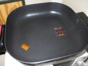
Second, my wife vetoed my use of the oven in the kitchen. This is completely understandable—we use it for food, and the hardware I’ll be heating, not being graded for food safety, could potentially produce all sorts of unfriendly gases and residues. This is a job for a garage oven, and that means a toaster oven. Fortunately, a fancy one isn’t necessary—an arbitrary box that semi-steadily holds its content at a set temperature is all we need. Much-Maligned Chain Department Store stocks a $15 firestarter model. They were out of stock, so I upgraded to the $20 firestarter model.

Supplies

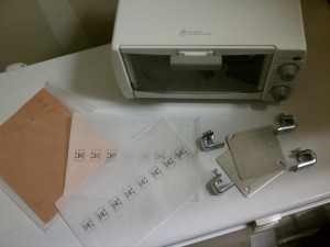
The ragtag bunch of misfits. Clockwise from top: Toaster oven, steel beam clamps, steel electrical work box cover plates, USB mini-B breakout board patterns on baking parchment, double-sided copper-clad PCB blanks.

So, on to the first experiments executed this evening.

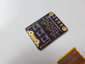
I started by printing the layout of Sparkfun’s USB mini-B breakout board several times over on baking parchment paper. I selected this board because it’s small and thus suitable for repeated trials. (As a bonus, I actually need one; I’ve got a couple of the connectors collecting dust in a drawer.)

Parchment

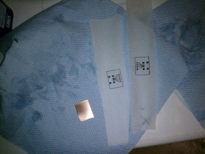
Left to right: A freshly cleaned piece of copper-clad, a nicely printed pattern on parchment, and one that didn’t come out so nicely.

Printing on parchment is tricky. It is something that you can get to work, but it may take a few tries. Parchment paper is coated with silicone, making it difficult to stick anything to. The fact that the paper releases easily is a desirable property for a toner transfer backing, but it does its job perhaps a little too well. Traces printed this way may not stick long enough to fuse correctly, resulting in smears and runs. When a pattern does take correctly, it must be handled somewhat delicately, as it can scratch or flake off without much of an impact. Still, since someone has gotten it to work[1], I think this can be a reasonably useful medium if you have some patience, and it’s certainly priced to sell (sold by the roll in your grocery store of choice).

I may include the other common media (magazine paper, inkjet glossy photo paper) in future experiments.

Incidentally, any sort of slick tape appears to be a bad choice for attaching the medium to ordinary paper; it being all I had at the moment, it caused more paper jams than I’ve ever encountered with this printer. I’ve had more success with matte tape[2].

I cut the copper-clad for the board and gave it a light cleaning with a soft abrasive[3] before building the apparatus around it.

Patterns, board, and one plate

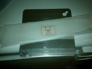
Copper-clad between two patterns on top of the bottom plate.

One copy of the pattern was placed on either side of the board. The registration wasn’t given too much attention because that isn’t the point of the current experiment (I’ll work on it once I have the adhesion process working), and because the patterns are both the same rather than flip sides of a double-sided board. To conserve the clearly printed copies of the pattern, a misprinted copy of the pattern was used on one side.

Apparatus with top plate

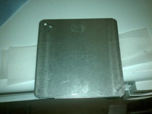
All of the above plus the top plate.

The board and patterns were laid down onto one of the steel plates, then the other plate was placed on top.

Apparatus with clamps

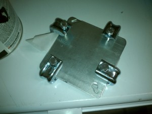
Clamps are added to press everything together.

The steel clamps were added to the edges of this sandwich and the bolts tightened.

Apparatus in oven

The smell of fresh-baked productivity. (But seriously, try not to inhale any fumes.)

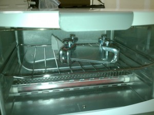
The full apparatus was then placed on the top rack of the preheated oven (there are two heating elements situated at the top and bottom, so the bake should be fairly even regardless) and baked for a specified amount of time.

Quenching the assembly

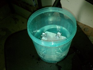
If lowered into the water slowly, there is audible boiling. If dropped quickly, as shown, you end up with a watery mess. Some sort of middle ground is probably a good idea.

Afterward, the assembly is removed from the oven and immersed in cool to tepid water, bringing it to a safe temperature for handling.

The results are examined immediately. The medium is removed without any special degree of care; any toner dislodged by normal handling cannot be considered to have adhered properly.

The variables I’m currently seeking to study are:

  • Bake time
  • Bake temperature
  • Clamp pressure

For tonight’s experiments, I decided on:

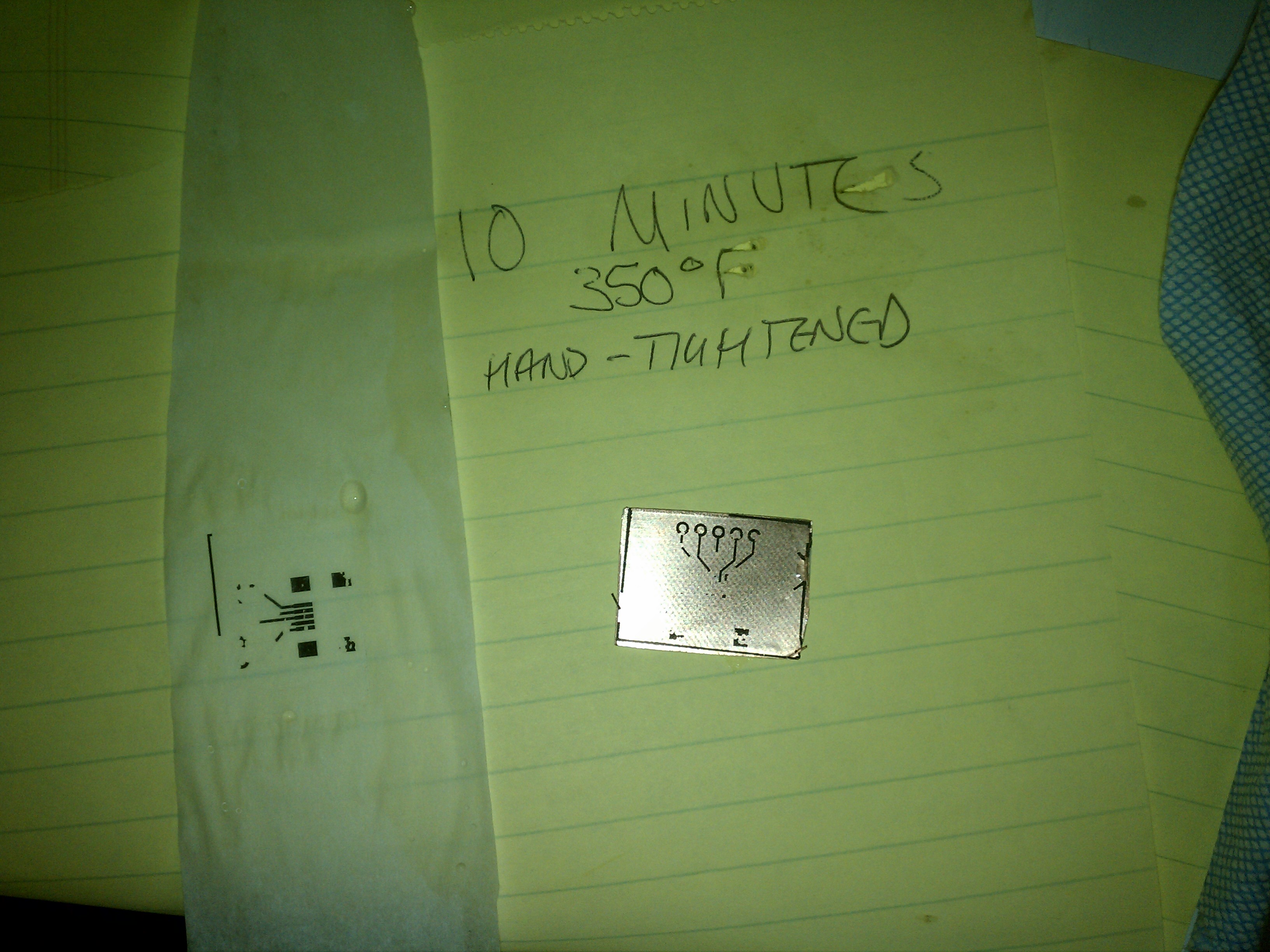
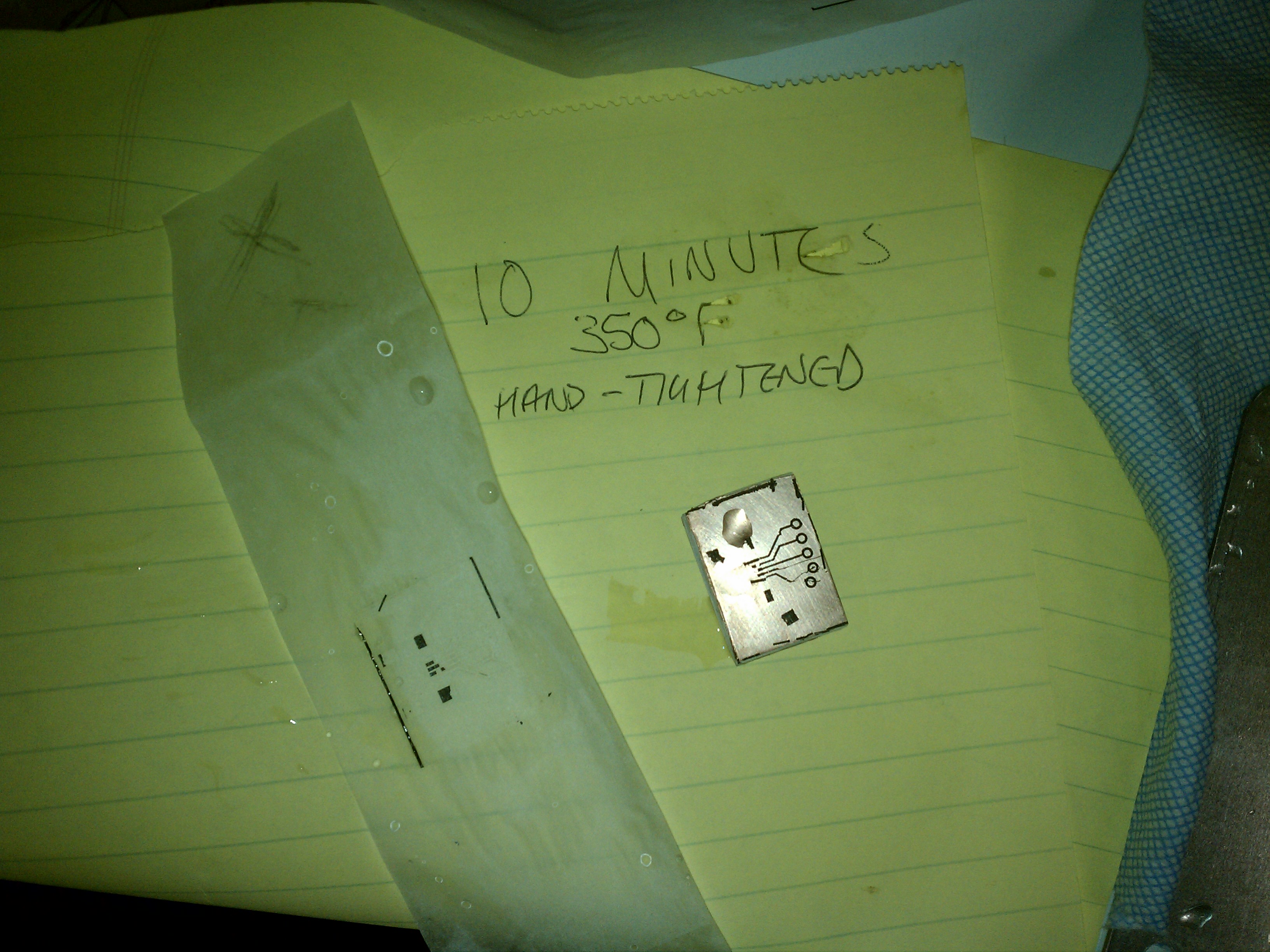
  • Trials of 10 and 30 minutes
  • Temperature of 350°F (setting of the oven, not measured temperature)
  • Clamp pressure resulting from tightening the bolts as far as I could using only my fingers, rather than a wrench.

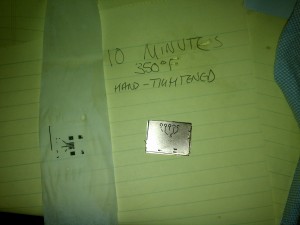
10-minute trial, proper side.

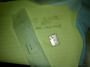
10-minute trial, misprint side.

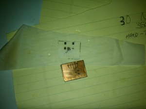
30-minute trial, proper side. Note that the extra time has discolored the copper somewhat.

30-minute trial, misprint side.

Put briefly, neither result was quite satisfactory, but I believe I’m on the right track. The 10-minute trial gave a better result than I’ve achieved with an iron and parchment. The 30-minute trial was somewhat better, but not so much so that I think adding more time is the key. The toner that did transfer was clear and crisp with no real smudging, which to me indicates that we could afford to apply more pressure. So, it’s likely that the next experiment will be a repeat of tonight’s, except using a wrench to tighten the clamps a little harder.

  1. [1]Refer to the Instructable by dustinandrews.
  2. [2]“magic” or “invisible” tape
  3. [3]Bar Keepers Friend soft cleanser.

While lying in bed last night, I was going over in my head everything I could recall having learned about getting a PCB[1] layout out of my computer and onto a piece of copper clad.

At this point in history I’ve managed to successfully iron a toner pattern onto a board only about three times, and each success came at the cost of around ten failures. The glossy photo paper is the only thing I’ve gotten to work; with magazine paper the image was too smudged to use, while with parchment paper hardly any of it stuck (though what did stick was high-fidelity). What has really been frustrating in this whole process is that there are too many variables and not enough correlation. I don’t know whether I haven’t been using enough pressure, waiting enough time, executing the correct motions, or using the right setting on the iron. For all I know, I could just have a crappy iron!

And everyone seems to have something different to try, with the most consistent results apparently from either (a) using a modified laminator for the toner transfer or (b) equipping for photoresist boards. Of the two, I would surely choose the photoresist, in part because it produces truly sharp results but mostly because the failure/success ratio seems to be lower. But both options involve buying new equipment (and in one case ruining it) with no guarantee of out-of-box success, and given the laser printer and copper-clads already in my possession, I’m already well in.

Anyway, I suddenly had an idea that, if it works, combines the even heat and pressure of a laminator with extremely low (new) equipment cost and increased controllability, the latter of which translates into more meaningful experiments and, when an experiment succeeds, more repeatable results.

What I decided was necessary is as simple as this:

  • The patterns are printed in reverse on the medium of choice—for me, it will be parchment paper since it already exists in my house.
  • The board is placed in alignment with the patterns on one or both sides.
  • The board and patterns are placed between two flat plates of rigid metal, such as steel.
  • The plates are bolted together and tightened at least to the point that nothing slides around.
    • Here, the sustained flatness of the plates is important so that the pressure remains fairly even across the entire pattern.
    • If you have any way to gauge it, take note of the tightness or pressure of the plates on the board. This is possibly one of the variables.
  • The oven is set to the target transfer temperature.
    • To be truly scientific about it, use an oven thermometer to ensure the knob is telling the truth.
    • The temperature is certainly one of the variables.
  • The oven is allowed to preheat until up to temperature.
    • My hypothesis is that a consistent result is probably easier to obtain from a preheated oven due to variances in rise time.
  • The plate apparatus is placed in the oven near the heat source.
    • If the apparatus can be hung sideways from the rack, do so allowing equal heat exposure to the two sides.
    • If the oven has a convection mode, it might be worth using.
  • A prescribed amount of time passes.
    • Another variable.
  • The apparatus is removed from the oven.
  • The apparatus is allowed (as by air) or forced (as by water) to cool to a safe temperature for handling.
    • Maybe another variable.
  • The apparatus is disassembled and the results are examined.
    • An effective transfer should stick well enough that it does not lift or flake when the medium is pulled away. Therefore, the medium can be pulled away without being exceedingly gentle.
    • If the result is unsatisfactory, a hypothesis is formed as to why that relates to one of the variables. The variable is adjusted and another attempt is made.

With this basic process in my head, I went to Chain Home Improvement Store to seek something I could use for the plates. What I found was square steel covers for electrical work boxes, in a flat variety with no punchouts. They already have holes for fasteners at two of the corners, and it was only $1 for the pair. I also got #10-24 stainless steel bolts and wingnuts which themselves totaled $4. This setup should adequately accommodate boards up to about 3 by 4 inches (for comparison, the standard Arduino footprint is 2.7 by 2.1 inches).

I now have all the equipment I think I’ll need to give this a shot, and that could happen as early as this weekend (and I’ll try to take photos). I really hope it works, not just because it would be convenient for me, but because it has the potential to lower the blood pressure of many other frustrated hobbyists.

  1. [1]printed circuit board
2-channel-power-Pch

If it works as intended, this circuit should allow an Arduino to control 2 different output voltages via PWM.

(EDIT: The above is the second revision.[1] Note also that the above will not work as-is, except perhaps in the NPN or N-channel variants; it doesn’t account for the fact that the op amp outputs peak well below the voltage necessary to turn off a PNP or P-channel transistor.)

Out of nowhere I just happened to find an 18V wall wart in my junk box. The lack of such a thing makes it necessary for a PIC programmer to produce its 12-14V programming voltage some other way, such as with an adjustable regulator and a pair of 9V batteries or with a boost converter. Even so, a programmer for production-quality output must be able to adjust its own programming voltage as well as its own output supply voltage.

Read More

  1. [1]This version uses P-channel MOSFETs instead of PNP, and better explains the power requirements.
piculear Suite

A suite of pieces that just might comprise a working PIC programmer when connected to an Arduino.

Years ago, while frustrated with my Microchip PICkit 2, which I only bought because of two failed attempts at building serial-port-based PIC programmer designs, I considered the possibility of a somewhat more open design that still had solid USB-based communications and the 5-to-13V boost converter, which was still kind of mysterious to me at the time.

Read More

This circuit provides a pulse-sequencing capability using the control voltage inputs of the 555.

The circuit described here triggers three (or an arbitrary number) monostables with differing but related widths. What’s different about this one than others I’ve seen is that this circuit has only one timing signal; in particular, there is only one RC network among all, which could potentially reduce the parts count and, more importantly, increase consistency among the timers.

The timing network is actually sort of a modified RC using a transistor and a voltage reference to charge the capacitor with a constant current. The timing is determined by the base voltage of the PNP transistor, the resistance at the emitter resistance, and the capacitance at the collector. The voltage drop across the resistor is the Vcc – Vb + Veb[1]. As long as none of these three values vary significantly in the application, the resistor’s voltage drop can be considered constant. If the resistor is, as expected, also constant, then the current through it is constant as well: I = V/R. The transistor will adjust as necessary, if possible, to maintain that current through the transistor[2]. If the supply voltage is well regulated, the base voltage can be set with a voltage divider.

The output of this constant current timing network, in contrast to the tricky curve of a regular RC network, is a linear ramp. This makes it easier to calculate the desired control voltage for each monostable. In the example above, the control voltages are 1V, 2V, and 3V, where the 1V and 2V timers produce a pulse exactly 1/3 and 2/3, respectively, the width of the 3V timer pulse. The values need not be this regular. A normal RC network could be substituted if you’re willing to do the math.

The monostable with the longest delay should have its discharge pin connected with its threshold pin in order to discharge the capacitor.

This approach gets a little unfortunate where setting the control voltages comes in. The CV is preset internally with a three-step resistor divider network. The CV itself is roughly 5k from Vcc and roughly 10k from ground. If I’ve done the math correctly, this is equivalent to a 2Vcc/3 supply through a 3.3k resistance. This means that you can’t trivially set the control voltage with a divider—something with a low (ideally zero) output resistance is necessary. Here are some things that might be worth trying:

  • Resistor divider with proper buffer (2 resistors, 1/4 to 1 op amp IC). If you’re not willing to complicate the calculations, an op amp can output the same voltage as the input, with no base-emitter drop. As a bonus, it’s an op amp, which is capable of a whole lot more. If restricted to Radio Shack, I’d pick up two TL082 JFET dual amps (or an LM324 quad if they’re out), then use three of the amps with a resistor ladder to set CVs and the one left over to upgrade the current source. I’d guess this is the option that would involve the least hair-pulling. (Edit: An example of a buffered resistor divider, complete with redone current source, in terms of a 7805 voltage regulator. Would require a supply voltage above 7 volts or so, but it’s an easy out in 2-3 ICs and about 10 resistors, plus the transistor and RC already in the circuit.)
  • Resistor divider with unity gain transistor (2 resistors, 1 NPN transistor). Similarly to the current source, the emitter voltage is a nearly fixed drop below the base voltage.
  • Trimmer (1 potentiometer, potentially up to 2 biasing resistors) if you’re okay with a bit of tuning.
  • Linear voltage regulators/references. Would probably work really well, but might be expensive depending on where you buy[3] and in this case requires a fairly small one (probably around 1V). The LM317 can be treated as a precision 1.25V drop, as long as the minimum load requirement is met.
  • Diode drops (1 diode). In the simulator, I was able to get the circuit to work with a ladder of diode drops for the control voltages (i.e., around 0.7, 1.4, and 2.1V). I’ve read that in practice this doesn’t work nearly as well.

By the way, the intended purpose is to trigger some D flip-flops to read serial data in an experimental line encoding I’ve conceived. It’s a variation of one I discussed way back, but the initial rising edge is followed by three bits of data before the mandatory fall. If it works, it could mean a simple output interface for PCs (e.g. via monitor or sound card) to devices that only understand data in terms of data, clock, and latch. What does this mean? You guessed it—semi-headless 74HC595 displays. (Okay, maybe not so much, but that’d at least be a good way to test it.)

This circuit is available on the Falstad simulator.

  1. [1]Veb may vary slightly depending on current, but is roughly 0.7V under normal circumstances.
  2. [2]Up to near the max collector voltage, in this case slightly lower than the emitter voltage.
  3. [3]LM317 is $3 at Radio Shack, but way cheaper online, especially in a TO-92 package.

No guarantees, but it worked in the simulator.

Today, figured out how to make a (possibly low-speed) transparent D latch out of an R-/S latch, plus a couple of logic gates, and an inverter. Each of these four things can be constructed from a 555 timer (or half of a 556). Alternatively, each of the gates can be replaced by three diodes[1] and a resistor, and the inverter by an NPN transistor and a resistor. Not pictured is the AC coupling[2] on the E input that would make this an edge-triggered flip-flop instead of a latch.

The significance of this is that a D flip-flop, a 1-bit static RAM and an important element of sequential logic, can be constructed very easily with stuff readily available from Radio Shack, which doesn’t stock logic ICs anymore but does carry 555s and 556s (as well as diodes, resistors, and transistors). Naturally, I have the best interests of the impatient experimenter in mind. :-)

  1. [1]With Schottky diodes you could probably get away with omitting the output diode.
  2. [2]In this case, an RC highpass is used, an inline capacitor of about 0.1µF followed by a 10kΩ pull-down resistor.