I’ve designed at least three or four different multi-74HC595+NMOS boards[1] over the past couple of years, but I believe this most recent one is the first one that ever worked on the first try.
Before I get to any specifics about that, here is a bit about how it was soldered.
Preflow
My technique has advanced since when I first experimented with plain solder reflow so many moons ago. I’ve developed this into a methodology I’m starting to refer to as “preflow” due to its relationship with reflow soldering. It’s nothing new and I even got the idea from multiple other sources, but I’d like to document the specific flourishes I’ve needed to apply to make it work for me.
We like reflow soldering because it’s an effective way to get SMT[2] parts attached correctly to a board, enabling us to perform the most delicate and error-prone task of initially positioning parts without heat (important to me because I have shaky hands and need the extra time).
Typically, solder paste and a solder paste stencil are used in the reflow process.
- Solder paste allows the placement of SMT components without the immediate use of heat.
- Solder paste is somewhat viscous and helps prevent the placed components from accidentally moving or becoming misaligned before the board is reflowed.
- A stencil precisely applies a metered amount of solder paste, which avoids excess solder that might cause bridging or imbalanced solder that might cause a component not to mount flush with the board.
- A stencil applies solder for the entire board, or even a whole panel of boards, in a single, very short pass, saving large amounts of time for production at any non-trivial volume.
But, as a hobbyist or for R&D purposes, perhaps we don’t care for solder paste or stencils.
- To use solder paste as recommended, we need to buy either a rather expensive small quantity or a larger quantity at a lower unit price. It does expire, so assuming we’re not producing in volume, the latter is no more economical. (Expired paste can reportedly be refreshed with the addition of some flux, but the result is a bit muddy and uneven compared to the fresh stuff.)
- Any significant leftover quantity must be refrigerated for longevity. This requires either a separate refrigerator or the willingness to keep a somewhat toxic, lead-based compound in proximity with things that need to remain edible.
- We’re not willing to waste money proactively ordering the stencil for a board design that we haven’t yet tested. (But solder paste without a stencil is a sticky, unworkable mess.)
This technique fills the roles ordinarily filled by solder paste and stencils with ordinary solder and paste flux. The main idea is to ensure that every pad has an appropriate amount of solder before placing the components.
- A soldering iron is used to apply solder to all pads. This puts solder everywhere it needs to go, like a stencil would. This part can be done quickly and imprecisely; the point is to ensure that no pad has too little solder.
- Manual soldering/desoldering techniques are used to remove excess solder and clear any bridging of adjacent pads.
- The board is “preflowed”: Flux is applied and the board is reflowed without any components in order to cause the solder to go, in so many words, where it goes when the board is reflowed. This step may seem superfluous, but it’s proven to be important. The preflow clears irregularities introduced by the manual process by redistributing and recentering the solder on the pads. This creates a sort of “print preview”, revealing any edits you might need to make to prevent bridging[3], dry joints [4], tombstoning [5], and so forth.
- If necessary, use manual soldering/desoldering to edit the solder, then repeat the preflow step.
- The solder now being in all of the right places, flux all the pads on board again using paste flux. The flux will be necessary for the reflow (as it is with solder paste, which has the flux already mixed in) and has a thick enough consistency to keep components from moving too much when placed.
- Place the components and reflow as normal.
The big con to doing it this way is the amount of time it takes; compared to paste and stencils it just does not scale at all. If I had to produce, say, 10 of the same well-tested module at a time it might be worth my while to gear up. But in my world, it’s usually new and untested design that I’m receiving in threes from Oshpark, and even having a stencil made doesn’t make any sense.
Ingredients
To do this stuff, you’ll need:
- A decent soldering iron. Mine is a Hakko FX-888. A cheaper one will probably do here, but a good iron is good for sanity.
- Copper cleaning wire for your iron (that is, the thing that looks like a copper scouring pad) or something else that will quickly and easily remove the excess solder from the tip of the iron.
- Accessories for desoldering by hand. At least desoldering braid/wick is pretty necessary for the subtler editing steps. A vacuum pump tool is useful for larger bits of excess solder.
- Ordinary flux-core Sn/Pb solder wire. (Lead-free might work, but I can’t vouch.)
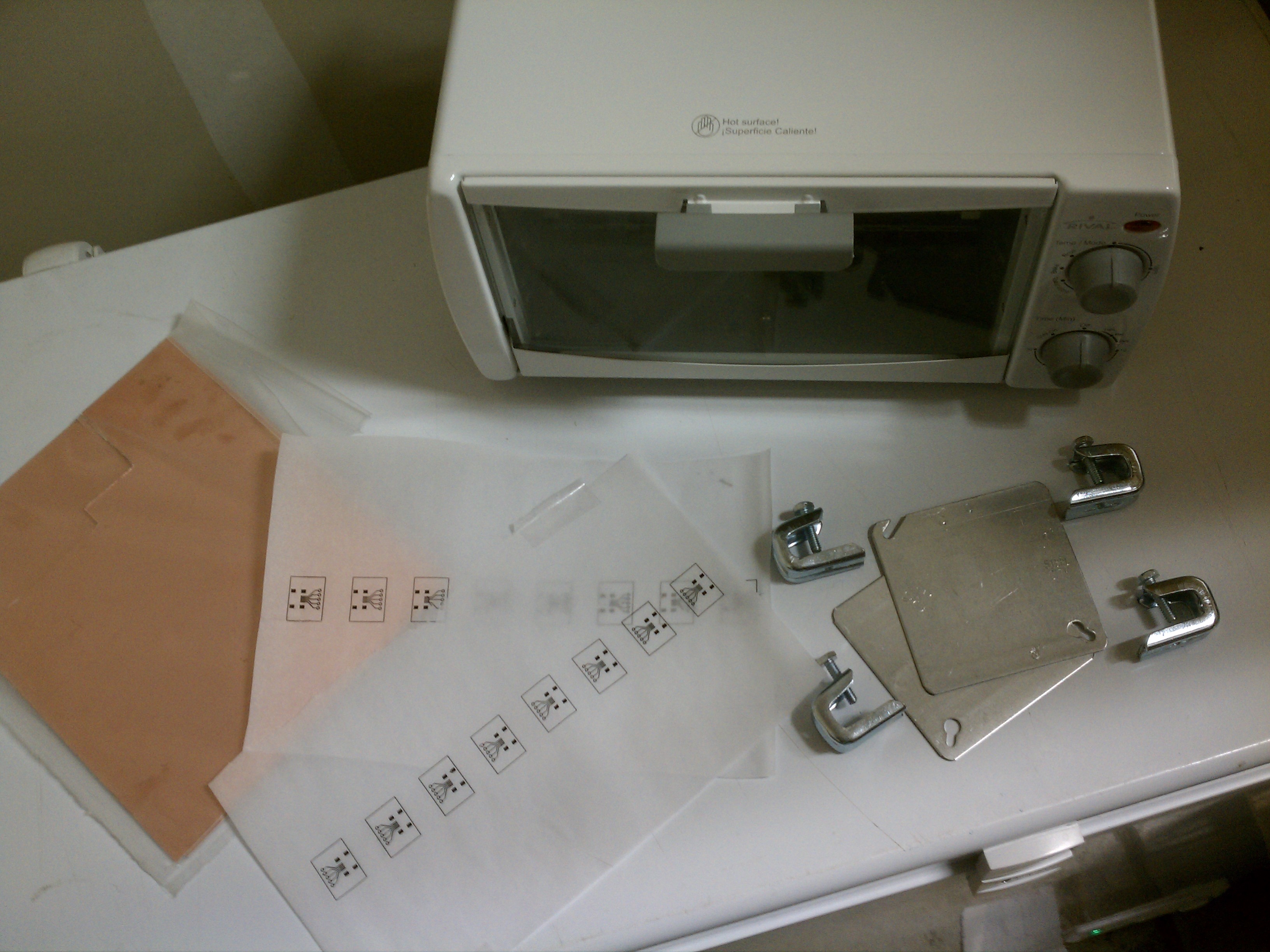
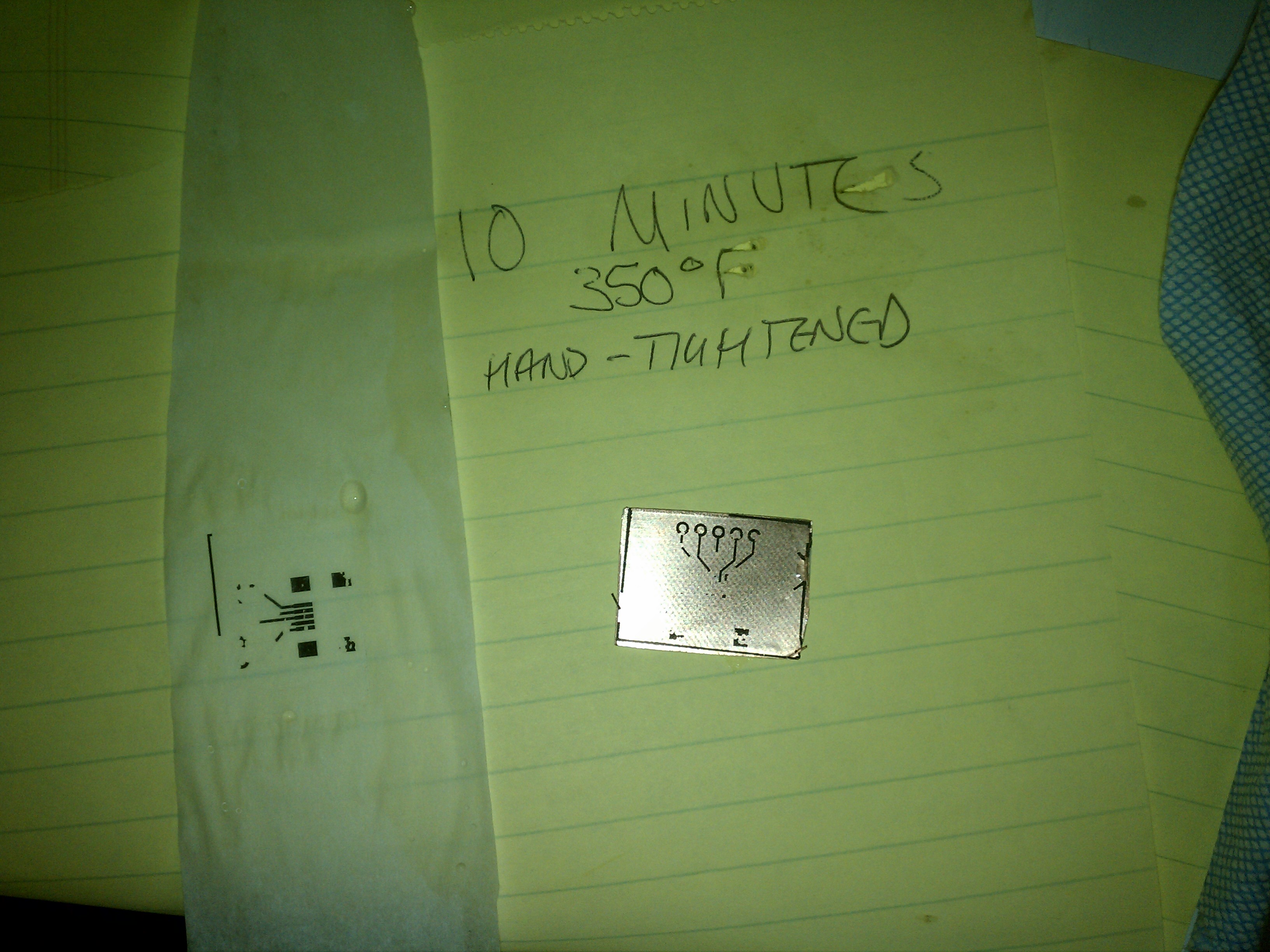
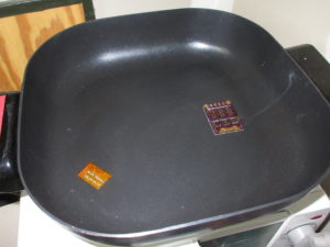
- Reflow oven or other apparatus for reflowing a whole board. I use a reflow skillet, just some Rival electric skillet, which I nominally set to 375°F (a little over 190°C).
- No-clean paste flux, for fluxing the pads just before placement. MG Chemicals 8341 is what’s on hand here. It must be paste; liquid flux won’t do here.
- A well-made PCB to receive the circuit.
- The board must include any solder mask that may be necessary. (Generally true for any reflow.)
- The current success follows on previous designs that experienced issues due to the solder mask clearance of a tiny SC-70 part not being tight enough to prevent bridging. This may be less of a concern if you aren’t designing your own footprints for parts like this.
- If you attempt to make homemade solder mask, make sure no part of it is flux-soluble. The previous article detailed how bad of an idea it is to try to use marker ink as solder resist. In a more recent experiment, stripboard with polyimide tape (“Kapton”) turned out to be a bad choice; the flux mixed with the tape’s adhesive and turned the board into a viscous piece of slop—and the result wasn’t even effective, leaving over half the board needing rework by hand.
- The pads must be the correct shape and size for the components. (Also generally true for any reflow.)
- This has also been a point of trouble for my homemade boards. Reflow soldering done on an appropriately made board helps components drift into position due to some surface-tension-related phenomena, but trying to get a 0603 resistor to stick correctly to a place I hastily scratched out for it from some stripboard didn’t go smoothly.
- The board must include any solder mask that may be necessary. (Generally true for any reflow.)
- Optionally:
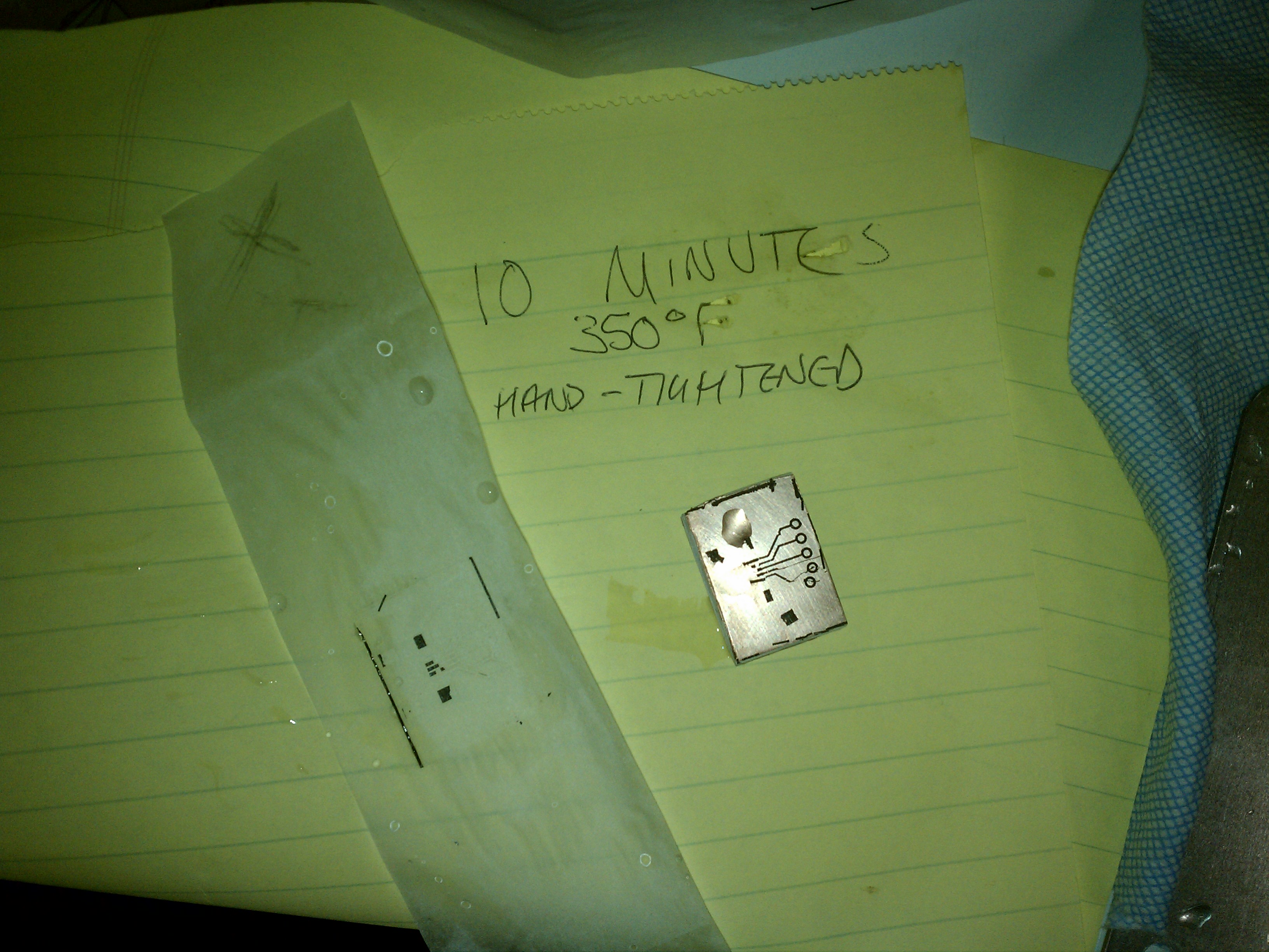
- A hot air rework tool. This doesn’t replace your reflow oven/device for the ultimate reflowing of the board itself—it produces an air current, which isn’t what you want after ten or twenty minutes of carefully placing components—but works nicely for the preflow phase. Mine is something I found on either Amazon or Aliexpress using the search term “858D”. One can still be had around $30, and it’s a purchase I don’t regret. It is always set to 350°C; there never seems to be any reason to change it.
- No-clean liquid flux. This doesn’t replace the paste flux for when you place the components, but for every other phase it’s a bit less messy (and just nice to have around for general-purpose soldering).
- Spray flux remover with a brush-tipped nozzle. All of the flux used here will leave the board tacky. This helps fix that. Isopropanol and ESD-safe cleaning brushes can also be used but tend to be a bit more work.
- A microscope or eye loupe for visual inspection. I picked up a product advertised as a 60X currency-detecting pocket microscope (it has white LEDs for plain illumination and a blacklight LED for verifying big bills) from Aliexpress for under $2. Very cheap, gets the job done, must recommend.
Editing
So far, editing the solder on the boards has involved clearing up these issues:
- Solder going where it shouldn’t or not going where it should. If the solder refuses to move in a way that is at all helpful, apply flux to the solder and pads and try again. (This turns out to be great advice for soldering in general. Flux is way more important than you might realize. Soldering without flux is masochism. Flux is the secret sauce to this whole activity.)
- Too little solder. A flat pad won’t properly attach to a component lead. Just add more solder.
- Too much solder. A pad with enough solder on it has a subtle, shiny dome. It shouldn’t look stuffed like a pillow. In general, if you brush off the iron tip, touch it to a pad, and then drag it away from the pad, it shouldn’t take (much) solder with it. Incidentally, this is also an okay way to correct the problem; take excess solder away with the iron tip, brush off the tip, and repeat.
- Way too much solder. If there’s anything on the board resembling a drop of solder, get rid of it. I use the vacuum tool for this one.
- That said, avoid using the vacuum tool for more delicate work. I’ve had the nozzle of a vacuum tool bend or scratch up pads and traces.
- Bridging between IC pads. If adjacent pads are sticking together, brush off the tip of the iron and then run it along the length of the pads in sort of a combing motion. If the iron isn’t picking up the excess solder even after brushing off the tip, there might be too much solder. The desoldering braid is useful here.
- Imbalanced pads. All pads for the same component should have the same amount of solder. If any pads have visibly different amounts of solder than the others, when reflowed they may fail to sit flush with the board or make adequate connections with all pins. Adjacent pads can be balanced somewhat by passing the iron across them repeatedly, which may take excess solder from one pad and deposit it on another. If the balanced pads ultimately contain too little or too much solder, see the previous advice.
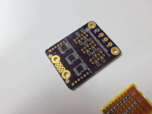
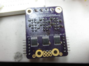
The mk 2, v1.10.1
Last August, I designed the most recent iteration of the board, but hadn’t assembled a copy until yesterday. (This module was to be part of a scoreboard feature for my family Fall Party, which for the past two years has featured game shows on stage, but I had to abandon the scoreboards and move on to the buzzers and other features closer to completion.)
Various problems had plagued the boards previously, and ultimately each byte would have a couple of non-functioning bits. The footprint I’d used for the SC-70 transistor packages had the solder mask set so loose that adjacent traces were exposed which tended to bridge easily. One pass had the transistor packages themselves adjacent rather than staggered, which caused the surface tension effects to draw one of them in between where two of them were supposed to go. Naturally, a well-designed board is important for reflow soldering, and this edition had removed all of the glaring errors.
Preworked.
The prework procedure described above resulted in a nicely pre-soldered board. The solder pads are all shiny and even-looking.

Pasted.
(Top: A syringe of paste flux. Left: A homemade stripboard masked with polyimide tape to demonstrate what not to do.)
The next step was to coat the exposed solder with paste flux in order to hold things in place and make the solder act in the way solder must.

Positioned.
Components are carefully put into place. Note the decoupling capacitor beside each IC being slightly off its mark. The two-contact components don’t sit quite stably on the domed tops of the solder pads. This isn’t a problem, though, because the surface tension effects of the solder will gently pull the component into place. This is actually kind of useful, as it provides a visual indicator that the reflow skillet has heated up enough to melt solder.
Piping.
The entire thing goes into the skillet to attach everything. If you look closely, you can see a bit of trouble.
 In the process of reflowing, one of the ICs and two of the transistor packages drifted slightly askew. Still, this sort of thing happens from time to time during reflow soldering, and out of 18 components, 3 isn’t that bad. I wonder if perhaps using less paste flux, or brushing it down to an even layer, would help prevent parts from floating off like this.
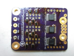
Proper.
With a little more flux, the hot air tool, and a minute or two of light nudging (it took surprisingly little time), the wayward components were restored to their proper places. Through-hole parts were added, a bit of Flux-Off removed the excess glop, and the device was ready. After attaching it to an Arduino and firing up a test sketch, much to my pleasant surprise—and I do mean surprise—it turns out all 24 bits are firing as they should. No going back with the continuity tester to find a mistake or anything. A true wonder!
- [1]74HC595, as you may or may not know, is a parallel-out shift register, which can be used to switch a large number of outputs over a small number of wires. Adding N-channel MOSFETs (sometimes known as “NMOS”) to the outputs allows them to drive higher current outputs.↩
- [2]surface-mount technology↩
- [3]Connection between adjacent pads or traces by a single blob, usually unintentional↩
- [4]Insufficient solder on a joint to make an effective connection↩
- [5]The habit of a usually 2-terminal component to stand up on one end after soldering, often caused by the effects of having a larger solder blob on one pad than the other↩