Archive

Data

A simple one-directional level shifter is easy to build out of an NPN transistor and two resistors in the common-emitter topology, if the application doesn’t need to sink as well as it sources—that is, if a significant output impedance is acceptable when the output is high. If low impedance is needed for high output, an additional PNP transistor and two resistors[1] can be added, again in common-emitter topology, to re-invert the signal, but then the output low has the impedance instead.

To both source and sink with comparably low impedances, the obvious solution, if you’re properly equipped, is probably CMOS: Two complementary MOSFETs configured to pull the output either up or down, with similarly low impedance either way—or, more likely, a CMOS logic IC that does the same thing, but in a more compact fashion.

Still, there are some possible issues:

  • If you don’t keep a stock of (fairly well matched) N-channel and P-channel FETs around, you can’t really build a CMOS inverter out of them.
  • If all you have are 74HC-series ICs, the output voltage must be from 2V to 6V. If your output voltage is, say, 13V, this is a no-go.[2].
  • If the input high voltage is too much lower than the output voltage, a logic high may not register properly. A preliminary low-to-high shifter (such as the single-sided NPN thing from before, 3 parts) would be needed for each input.
  • If the input high voltage is too much higher than the output voltage, a logic high may do some damage to the IC. A preliminary high-to-low shifter (such as a resistive divider, 2 parts) would be needed for each input.

Incidentally, constructing a CMOS-like complementary output using discrete bipolar transistors is not advisable;  even short input transitions can cause high and low transistors to be on simultaneously for a non-trivial amount of time, a condition called shoot-through, which results in a massive current spike likely to damage both transistors and possibly other components. One way to avoid this condition is to add a resistance between the high and low sides, but then we’re back to the original problem. Shoot-through is evidently less of a concern with CMOS, partly because the FETs involved have better tuned and matched thresholds, and partly because a MOSFET is less subject to self-destruction via thermal runaway than a BJT.

Wanting to prototype something with an oddball push-pull 3.3V-to-13V switch led me to concoct an experiment using only stuff available at a reasonably well-stocked Radio Shack[3], with particular attention to ICs that provide push-pull outputs. So far I’ve tried configurations based on the original 555 timer[4] and the TL082 op amp.

My first experiments with the TL082 in Schmitt trigger configuration were not promising, but I’m suspicious something may have been connected wrong; the logic low never went below 1.15V, which happens to have been the reference voltage, half of 3.3V. Either way, the supply voltage had to read 17.3V for a high output of 13V.

In contrast, the 555-based Schmitt trigger appears to be a workable solution, as long as you can drive the chip 1.5V higher than the desired high output.
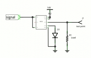
555 shifter

555 as a level shifter in just two parts (not including the load). Output is a roughly fixed amount below Vcc.

The output stage of the 555 is a push-pull output, but it is implemented with bipolar transistors in a traditional style, meaning both high and low sides are NPN transistors. This works, but at the cost of about 1.5V from Vcc. If you can pay that cost, it should work nicely.

In my experiments with the pictured circuit, using 1K for the load, the output was 12.5V for a 14.0V input. Similarly, it went up to 13.0V for 14.5V input, and 5.0V for 6.5V.

Apart from the 555, there is a diode to set the control voltage. The CV pin is essentially the top split of a 5K:5K:5K resistive divider from Vcc to ground. The splits of this divider set the high and low thresholds of the Schmitt trigger; they are CV (default 2Vcc/3) and CV/2, respectively. A silicon rectifier diode is added from the CV pin to ground, forming a crude shunt regulator with the internal resistors. This sets CV to about 0.6V and the low threshold to about 0.3V. This is suitable to make the input accept a clean signal directly from a 3.3V or 5V CMOS logic output. Adding a second diode in series with the first would double those levels, making input from a somewhat noisy source or from 5V TTL practical. CV could similarly be set using a Zener diode (in reverse) or by constructing a voltage buffer, but at that point you may just want to order a more suitable part.

So, there you have it—an imperfect but still practical low-impedance level shifter in just two parts.

  1. [1]or one resistor, with caveats I haven’t fully investigated
  2. [2]If you have the older CD4000-series ICs, however, up to about 18V is possible, as long as the inputs are brought within range.
  3. [3]For those of us who don’t have 24 hours to wait for progress.
  4. [4]Not the TLC555 they also carry, which may work better or worse.

I’ve been spending a lot of time thinking about op amps and comparators lately.

One of the common uses of an op amp is as a “unity gain” buffer, meaning that the output voltage is as close as possible to being the same as the input voltage. At a glance this might seem like a trivial thing, but it’s used to great advantage.

For example, a resistive voltage divider can be used to derive some fraction of a larger voltage by representing the ratio with resistors. Given a 9V supply, a divider over 100K and 47K would yield about 2.9V (9V * 47K/(100K+47K)). Unfortunately, this is of only limited use directly, since driving a load from the output causes that voltage to drop. This happens because the load itself acts as a resistor to ground in parallel with the divider, changing its resistance.

The divider does okay, though, feeding to a high-impedance input (i.e., one that doesn’t pull a lot of current). The inputs on an op amp fit that description, and its output is low-impedance (meaning that it can supply current without trouble). That’s a huge part of why op amps are useful. If you take the resistive divider’s output into the non-inverting (“+”) input of an op amp and the amp’s own output into the inverting (“-“) input, you get a unity gain buffer, an amplifier that outputs the same amplitude as the input (“unity gain” refers to the 1:1 ratio of input to output). The buffer continuously compares its output to the input. If the output is too high, it’s lowered; if too low, it’s raised.

In general, the op amp’s job is to perform an analog computation on its inputs that amounts to subtraction followed by multiplication. It subtracts the voltage of the inverting input from the voltage of the non-inverting input, then multiplies it by a factor called gain. By default, the gain is an arbitrarily high number called the open-loop gain of the amp. However, by feeding the output back into the inputs in different ways, it’s possible to fix the gain to a more useful value, such as 1 in the above scenario.[1]

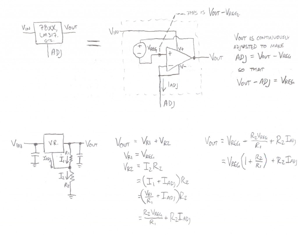
Anyway, this ability to continuously adjust an output to a certain point reminded me of linear voltage regulators, like the 7805 and the LM317. I hypothesized that these 3-terminal regulators are basically heavy-duty op amps with a fixed voltage reference on one of the inputs. A little research confirmed this.

A linear voltage regulator is a voltage reference stuck to an op amp with high output current capability. Now you know—and knowing is half the battle.

[Note: The above image replaces a previous version that was less accurate.]

The data sheet for the fixed 7805 (and other 78xx) regulators suggested a circuit that allows the use of the regulator in an adjustable mode for voltages higher than the nominal voltage. Under normal circumstances, the regulator simply adjusts the output pin to be exactly 5V above the ground pin. In this mode, the ground pin is not tied to ground. Instead, the output and ground pin are placed across the high side of a resistive divider. The regulator fixes the voltage across the upper resistor to its face value. The lower resistor gets all of the current from the upper resistor, plus the garbage quiescent current from the machinery in the device. Multiplying this sum by the lower resistance yields, via Ohm’s law, the voltage across the lower resistor. The sum of that voltage and the regulated voltage is the output.

The data sheet for the LM317 shows a circuit essentially identical to the one described above with a few name changes. In fact, the ‘317, when used in the 7805’s nominal configuration, is itself a fixed 1.25V[2] regulator.

Knowing that these regulators are so alike, then, why should we ever choose ‘317 over 7805? The answer: ‘317 has a subtle difference that makes it far more suitable in its adjustable mode: The current out of its adjustment terminal is a couple of orders of magnitude smaller[3], enough smaller in fact that it could be disregarded in many cases when calculating Vout. This is especially useful in cases where the application doesn’t adjust the output voltage, but that requires a regulator for an awkward voltage (like the 13V programming voltage of a PIC). Using a 7805 in such an application might require a trimmer to fine-tune the output, while the ‘317 would probably be okay with a fixed-value resistor instead.

Pictured are the much simplified equivalent schematics, plus my derivation of how Vout is calculated. R2Iadj should be dominated by the rest of the expression.

  1. [1]Incidentally, a comparator is basically a specialized op amp that has been optimized to only output high or low (i.e. in the logical sense). It works as specified above, but boils the problem down to “is the non-inverting input greater than the inverting input?” yielding high if so and low if not. An op amp can be used as a comparator, but actual comparators do the job faster and better.
  2. [2]1.25V is less arbitrary than you might think: It is the output of a silicon bandgap reference, which is designed to be steady and reliable in spite of temperature and environmental changes. Cool.
  3. [3]7805 IQ is 5mA typ., LM317 Iadj is 50µA typ.

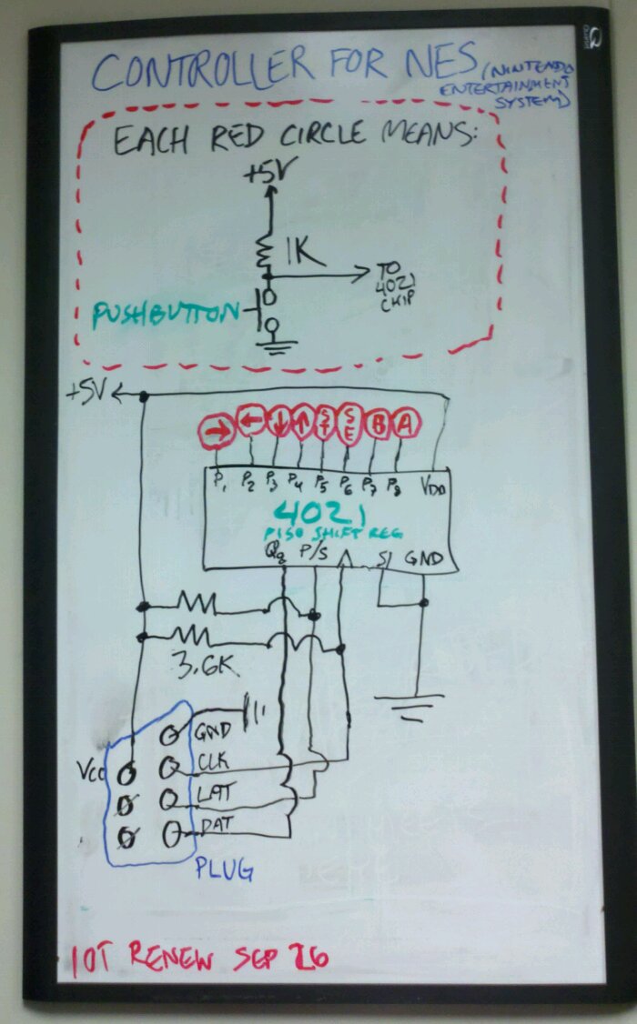
See also a previous post about game controller signaling.

A Serious Serial Protocol: Sony PlayStation and PlayStation 2

  • Number of pins on connector: 9 (proprietary male)
  • Number of inputs to encode: 14 on the original gamepad (up, down, left, right, select, start, BT/”triangle”, BO/”circle”, BX/”cross”, BS/”square”, L1, L2, R1, R2), but arbitrarily more, including analog inputs
  • Mapping strategy: One pin for all inputs
  • Reading strategy: A fairly comprehensive full-duplex serial protocol, including provisions for acknowledgement and additional instructions sent by the system, similar to and probably compatible with SPI
  • Number of pins used: 8 = 3 power (1 ground, 1 logic supply of nominally 3.3V but possibly more[1], 1 rumble motor supply of nominally 9V but generally closer to 7[1]) + 2 data lines (1 CMD from system, 1 DAT from controller) + 3 signaling lines (1 ATT from system, 1 CLK from system, 1 ACK from controller). (Actual pin names vary.) One pin is left unconnected.
  • Fun fact: The same protocol (with different headers and commands) is also used for memory cards.

Sony’s system uses a serial protocol, as was the case with Nintendo, but the Sony version is somewhat more flexible—and quite a bit heavier. As described elsewhere, while it’s possible to implement this protocol using standard logic chips, it takes six of them just to implement the original controller[2]. This protocol very much assumes the presence of at least a microcontroller (which is okay—they’re pretty cheap, and replacing hardware with code often has some serious advantages).

Electrically, the controller ports form a bus. With the exception of the ATT line, all lines are shared among all nodes. The lines that are input into the system, ACK and DAT, are open-collector inputs (to put it one way, instead of “low” or “high” the line expects “low” or “nothing”), allowing them to be shared across devices. The system addresses one controller at a time by lowering the ATT line for that controller.[3] It would make sense for a controller to tri-state ACK and DAT whenever ATT is not low.

When ATT drops, a new session (or packet[1]) begins, and the system and controller prepare to exchange data 1 byte (where a byte is 8 bits in little-endian order) at a time. The controller outputs data on the DAT line and accepts input from the system on the CMD line. Both lines are clocked from CLK. The data lines are set up on a falling edge and read on a rising edge. After each 8 bits, the controller acknowledges receipt by pulling ACK low for a short time[4] The last byte of a session shouldn’t be ACKed; if the hardware tri-states when ATT is off then the ACK pulse wouldn’t be output anyway.

The number of bytes in the session depends on the content of the session itself. The system starts by clocking three bytes: 0x01 (start session), 0x42 (poll), and an idle byte (0xFF). At the same time, three bytes are received from the controller: an idle byte (0xFF), a 1-byte controller ID (such as 0x41 for the original gamepad), and then 0x5A (“here comes data”). (If the ACK is not received after any byte, the system considers the connection broken and moves on.)

The amount of data that comes afterward depends on the controller ID. A digital gamepad yields 2 data bytes (encoding 14 buttons in 16 bits), the classic analog is 6 bytes (the same as digital, plus L3 and R3 stick triggers and 8 bits each for LX, LY, RX, and RY), and, on the PS2 using DualShock 2, a whopping 18 bytes: 6 bytes as with the original analog, plus an 8-bit pressure level for each of the main 12 action buttons!

It’s also possible to send other commands to the controller. Among them is a sequence of commands that can be used to allow some of the idle bytes in the 0x42 command to be used as levels for the vibration motors.

(Sources: [1],[2])

  1. [1]http://store.curiousinventor.com/guides/ps2/
  2. [2]http://www.gamesx.com/controldata/psxcont/psxcont.htm
  3. [3]ATT roughly corresponds with the NES latch line OUT 0, but is active-low and stays low for the duration of the session.
  4. [4]Sources conflict as to exactly when and for how long, but it’s on the order of one cycle width on CLK. The standard logic version mentioned before uses a missing pulse detector on the CLK line since it goes idle between bytes. It’s probably not too sensitive either way.

♫ SEEEEEEEEEGAAAAAAAAAAAAAAA!!! ♫

Ahem.

To complement my previous post, here is a schematic of the regular Sega Genesis controller. You could actually make one of these from scratch from non-specialty items; unlike the NES controller, which uses a proprietary 7-pin connector, Sega used the common-as-dirt DE-9 female D-sub connector, following in the footsteps of Atari both physically and electrically.

The circuit above could be built in fairly little time using almost exclusively items from RadioShack, if it’s well stocked. There’s probably still a DE-9 connector kicking around there. You’re not likely to find a 74HC157 in a local store, but it’s easy enough to make a 2-1 mux using 74HC00 quad NAND ICs. If you can’t track those down, it appears to be possible to make a non-inverting 2-1 mux in as few as 9 or so transistors (probably MOSFETs), but my personal recommendation, which is more time-intensive but overall less masochistic, is to have a working stock of a key few 74HC-series ICs available for when you get curious.

If I were to do it this way, I’d pull a couple of 74HC00 from my stash. A 2-1 mux—let’s call it MUX(M,N,S)—implements the expression MS OR N(NOT S); that is, “reflect M if S is high; reflect N if S is not high”. That’s equivalent to the expression (M NAND S) NAND (N NAND (S NAND 1)), which is four NAND gates. One 74HC00 = 4 NAND gates = 1 mux.

A 74HC157 packs four of these, but only two are genuinely in use. Most game software probably ignores the left and right signals while the select line is low, so it’s most likely okay to pass the left and right buttons directly out pins 3 and 4 of the port (as is already the case with up and down). As for the rest, pin 6 would be MUX(A button, B button, select) and pin 9 would be MUX(start button, C button, select).

Of course, as if it even bore mentioning, this controller would be a cinch to implement on an Arduino-like platform using just a DE-9 breakout cable. (Hint: Vcc on pin 5, ground on 8, an input on 6, and the rest are outputs.) Do this only on a temporary basis, though—you have better things to do with an Arduino. :-)

A couple of weekends ago I found myself in conversation with Jon, my brother-in-law, a vintage game systems collector and proud owner of an Action 52 cartridge, about NES controllers—specifically, how all eight buttons can be crammed down only seven controller pins (a trivial setup would require nine). I just happened to know most of the mechanism already and gave him the surprisingly simple rundown. I got curious about the parts I didn’t know, so here’s a digest of my research.

Read More

Do you get a lot of use out of the scroll wheel on your mouse? How about that Griffin PowerMate you got for your birthday? If so, chances are that rotary encoders are responsible for some of the joy in your life.

15-period code wheel

A 15-period code wheel for a rotary encoder. Believe it or not, this hypnotic image is an important part of an analog-digital converter! Generated using the script at the end of this post.

Read More

In the previous post, I believe I dismissed Manchester coding too quickly as a possibility, thinking that some unwieldy analog circuitry would be necessary for its implementation. Today, I realized that it would actually be fairly easy to create a decoder using microcontroller code that would fairly easily handle arbitrary bitrates and even possibly do a decent job accounting for drift.

To explain, Manchester coding is a type of self-clocking signal (i.e., it combines data and clock lines) that guarantees either one or two edges (transitions from low to high or high to low) per bit. A logical 0 starts high and then switches to low mid-bit; a logical 1 goes low to high instead.(Described above is the IEEE version. As the image shows, it’s possible to flip the two by convention.)

What the microcontroller must do to make sense of such a signal is pretty simple, much to my delight. It’s simple because there are only two possibilities for the duration between transitions; we’ll call them D/2 for the narrow pulses and D for the wider ones. Assuming we have a decent guess at what D is (we’ll get to that), and that any two consecutive D widths are reasonably similar, we can decode the pulse train and even compensate for gradual drift of the D value. It goes something like this:

  • Say we have 3 initial guesses for D, which are D0, D1, and D2. At any given moment, our estimated value of D = (D0 + D1 + D2)/3.
  • At each transition, find X, the distance between this and the previous transitions.
    • If X < (3/4)D, consider X to be approximately D/2. Ignore this transition and start waiting for the next one.
      • If 4X < 3D then X < (3/4)D. 4X = X shifted left 2. 3D = D0 + D1 + D2. No actual multiplication or division required!
    • If (3/4)D ≤ X < (3/2)D, consider X to be approximately D. Accept the current input as the next bit. Let D0 = D1, D1 = D2, D2 = X.
      • If 2X < 3D then X < (3/2)D. 2X = X shifted left 1. 3D is as above.
    • If X ≥ (3/2), the transmission has ended or there is an error; handle accordingly.

Using this mechanism, the average of the previous three bit widths is used as the expected width for the next bit, but the next bit can be nearly 25% narrower or 50% wider and still be valid. Since this sliding window approach is used, the bitrate could generally vary by quite a lot as long as the change is gradual. Oversampling is key here—I imagine that the receiver should try to sample at least 6 times (wild guess) the expected bitrate.

How do we set up initial guesses for D? Here’s one proposition on how to make an explicit initial sync:

  • The initial guess for D would be very short, possibly shorter than any actual expected D.
  • When the line is idle, it is held low, and should be held low longer than the max nominal 2D specified by the system. Consequently, if the line is low for over twice the expected 2D, the receiver should recognize an idle state.
  • When a frame is about to be sent, the line goes high for exactly X = 2D as decided by the sender. At the next high-low transition, the receiver assigns D0 and D1 based on this value: D0 = X shift right 1; D1 = X – D0.
  • The transition following this transition is the start bit, which is a 1 (low-to-high). The width Y of the low before the transition is approximately D/2. Assign D2 based on this value: D2 = Y shift left 1.
  • Start sampling as specified from the start bit transition.
  • After some fixed number of bits, the frame ends with a stop bit, which is a 0 (high-to-low). After the bit, the line is held low to indicate idle as mentioned before.

This one’s got some true promise, I think. I’m guessing it may even be possible to get it working using a high-tolerance clock on the slave micro (such as an RC network) making it potentially feasible to use even a super-cheap one, like the PIC16F54 of which I happen to have plenty lying around, without an excessive amount of tuning. I could be wrong, though. Who knows?