Concept: Push and Pull

This circuit has not been tested. It might work. It might not. Who knows? All diodes should probably be Schottky.
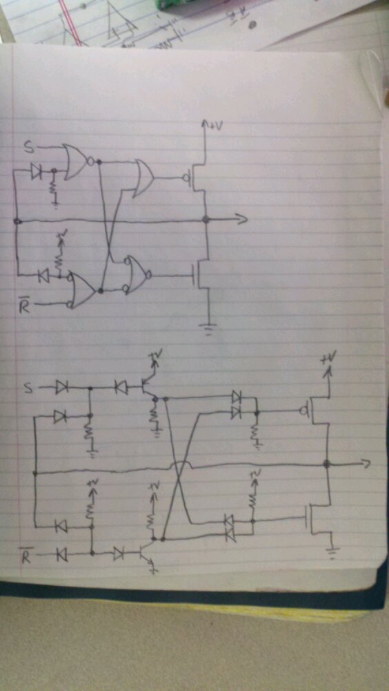
I contrived a diode-transistor logic (DTL) circuit for a SR latch[1] with a CMOS push-pull output and a break-before-make mechanism to prevent simultaneous push and pull (shoot-through). I have no idea whether it actually works and there are probably easier ways to do it, but it was kinda fun.
The upper schematic lays out the concept in terms of OR gates with different inversions (clockwise from upper left: NOR, OR, AND, NAND). The output is fed back into the inputs through diode-resistor level shifts so that the one being fed into the high side is high when the output is high but low if the output is either low or off (high-impedance), and the one into the low side is low when the output is low, but high if the output is high or off. This feedback should prevent either output FET from turning on until the complement is turned off (or close to off).
The lower schematic is the upper schematic rendered in diode-transistor logic. The lower-left gate, a NAND, is implemented using the textbook DTL NAND with an NPN transistor. The NOR in the upper left is actually the same as the NAND, but with the diodes reversed and a PNP on the output. Note that in both cases the feedback diode-resistor shift is now part of the gate itself. The other two gates are just diode logic since OR (upper right) and AND (lower right) can be implemented without a transistor on the output.
This contrivance is for a power logic buffer; the intended supply voltage would be somewhere from 12 to 48 volts and the current capacity on the output MOSFETs would be at least a couple of amps. I haven’t tested the thing. Please don’t use it, except in test circumstances, unless you know what you’re doing.
- [1]Technically, an S AND NOT R latch.↩