No guarantees, but it worked in the simulator.

Today, figured out how to make a (possibly low-speed) transparent D latch out of an R-/S latch, plus a couple of logic gates, and an inverter. Each of these four things can be constructed from a 555 timer (or half of a 556). Alternatively, each of the gates can be replaced by three diodes[1] and a resistor, and the inverter by an NPN transistor and a resistor. Not pictured is the AC coupling[2] on the E input that would make this an edge-triggered flip-flop instead of a latch.

The significance of this is that a D flip-flop, a 1-bit static RAM and an important element of sequential logic, can be constructed very easily with stuff readily available from Radio Shack, which doesn’t stock logic ICs anymore but does carry 555s and 556s (as well as diodes, resistors, and transistors). Naturally, I have the best interests of the impatient experimenter in mind. :-)

  1. [1]With Schottky diodes you could probably get away with omitting the output diode.
  2. [2]In this case, an RC highpass is used, an inline capacitor of about 0.1µF followed by a 10kΩ pull-down resistor.

Younger hobbyists who want to do arithmetic in an electronics application may think that a microcontroller is the only way to do it. I present something far more old-school.

image

How to do simple math on real numbers in a very non-digital way.

If you can represent the scalar terms of an arithmetic expression as voltages and/or resistances, then many operations can be performed with op amps (which is, incidentally, what the “op” part means). Several of the major features are described above.

  • The word “amp”, for amplifier, refers to the fact that the device amplifies, or enlarges, an input signal by a factor called gain which is represented by the letter A[1] When A is fixed, the amplifier serves to multiply the input signal by A. By default, A is ideally infinite[2], but can be set to a fixed value using resistors.
  • Division (not pictured) can be performed using a resistor divider network. No op amp is required, though using one might be desirable to avoid loading effects.
  • “Subtract then multiply by A > 0″: An op amp’s natural mode (in my opinion, anyway) is the differential amplifier. Two voltages are input; V2 is subtracted from V1, and then the difference is multiplied by A, which is based on the ratios of resistors used. All other linear modes pictured can be described in terms of this one:
    • “Multiply by A >= 1″: If you take the divider off of V2 and replace it with Vin, it’s equivalent to setting V2 to Vin(1 + Rin/RF). Then, just set V1 to 0. The result is A(V2V1) = (RF/Rin)Vin(1 + Rin/RF) = Vin(1 + RF/Rin).
    • “Multiply by A < 0″: Let V2 = 0, V1 = Vin. The result is A(V2V1) = (RF/Rin)(0 – Vin) = Vin(-RF/Rin).
    • “Add then multiply by A < 0″: Exactly the same as the previous case, except that the input is from a resistor divider network. If V1 and V2 are fed to the same point through equal resistances as shown, it’s equivalent to a single input of VX = (V1 + V2)/2 through a resistance of RX = Rin/2. With the other input at 0, the result is A(0 – VX) = (RF/RX)(-VX) = -(2RF/Rin)((V1 + V2)/2) = -(RF/Rin)(V1 + V2).
  • “Logarithmic” and “Exponential”: An NPN transistor with a grounded base can be placed either at the feedback or the input to implement a logarithmic or exponential output, respectively. The coefficients of the expression are not well defined, since they vary from instance to instance, but if the transistors used are closely matched and thermally linked (for example, in a single-chip transistor array) then with some tuning their outputs will be consistent. A log transform can be used to easily multiply (by adding logarithms) or divide (by subtracting logarithms) two voltages.
  • Comparison (not pictured): As discussed here previously, a comparator is a sort of op amp specialized to output only logical high/low depending on whether the value at the non-inverting input is higher than the value of the inverting input, outputting high and low, respectively. In a pinch, an op amp will do the same thing in the open-loop configuration—direct inputs and no feedback, resulting in the extremely high gain mentioned earlier. If the non-inverting input is even slightly different than the inverting input, that small difference is amplified so immensely that the output will be either the highest possible or the lowest possible, meaning around the positive and negative supply voltages, respectively. Use of an actual comparator is preferred though, since it is better tuned for digital use.
  1. [1]The “A” presumably refers to “amplification”.
  2. [2]But in practice is just a very high number.

This circuit has not been tested. It might work. It might not. Who knows? All diodes should probably be Schottky.

I contrived a diode-transistor logic (DTL) circuit for a SR latch[1] with a CMOS push-pull output and a break-before-make mechanism to prevent simultaneous push and pull (shoot-through). I have no idea whether it actually works and there are probably easier ways to do it, but it was kinda fun.

The upper schematic lays out the concept in terms of OR gates with different inversions (clockwise from upper left: NOR, OR, AND, NAND). The output is fed back into the inputs through diode-resistor level shifts so that the one being fed into the high side is high when the output is high but low if the output is either low or off (high-impedance), and the one into the low side is low when the output is low, but high if the output is high or off. This feedback should prevent either output FET from turning on until the complement is turned off (or close to off).

The lower schematic is the upper schematic rendered in diode-transistor logic. The lower-left gate, a NAND, is implemented using the textbook DTL NAND with an NPN transistor. The NOR in the upper left is actually the same as the NAND, but with the diodes reversed and a PNP on the output. Note that in both cases the feedback diode-resistor shift is now part of the gate itself. The other two gates are just diode logic since OR (upper right) and AND (lower right) can be implemented without a transistor on the output.

This contrivance is for a power logic buffer; the intended supply voltage would be somewhere from 12 to 48 volts and the current capacity on the output MOSFETs would be at least a couple of amps. I haven’t tested the thing. Please don’t use it, except in test circumstances, unless you know what you’re doing.

  1. [1]Technically, an S AND NOT R latch.

I’ve been spending a lot of time thinking about op amps and comparators lately.

One of the common uses of an op amp is as a “unity gain” buffer, meaning that the output voltage is as close as possible to being the same as the input voltage. At a glance this might seem like a trivial thing, but it’s used to great advantage.

For example, a resistive voltage divider can be used to derive some fraction of a larger voltage by representing the ratio with resistors. Given a 9V supply, a divider over 100K and 47K would yield about 2.9V (9V * 47K/(100K+47K)). Unfortunately, this is of only limited use directly, since driving a load from the output causes that voltage to drop. This happens because the load itself acts as a resistor to ground in parallel with the divider, changing its resistance.

The divider does okay, though, feeding to a high-impedance input (i.e., one that doesn’t pull a lot of current). The inputs on an op amp fit that description, and its output is low-impedance (meaning that it can supply current without trouble). That’s a huge part of why op amps are useful. If you take the resistive divider’s output into the non-inverting (“+”) input of an op amp and the amp’s own output into the inverting (“-“) input, you get a unity gain buffer, an amplifier that outputs the same amplitude as the input (“unity gain” refers to the 1:1 ratio of input to output). The buffer continuously compares its output to the input. If the output is too high, it’s lowered; if too low, it’s raised.

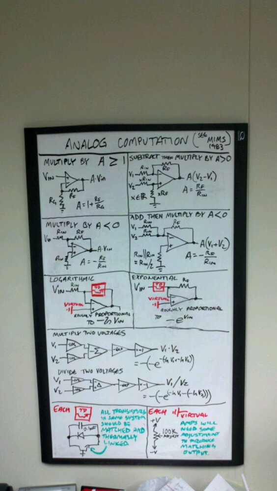
In general, the op amp’s job is to perform an analog computation on its inputs that amounts to subtraction followed by multiplication. It subtracts the voltage of the inverting input from the voltage of the non-inverting input, then multiplies it by a factor called gain. By default, the gain is an arbitrarily high number called the open-loop gain of the amp. However, by feeding the output back into the inputs in different ways, it’s possible to fix the gain to a more useful value, such as 1 in the above scenario.[1]

Anyway, this ability to continuously adjust an output to a certain point reminded me of linear voltage regulators, like the 7805 and the LM317. I hypothesized that these 3-terminal regulators are basically heavy-duty op amps with a fixed voltage reference on one of the inputs. A little research confirmed this.

A linear voltage regulator is a voltage reference stuck to an op amp with high output current capability. Now you know—and knowing is half the battle.

[Note: The above image replaces a previous version that was less accurate.]

The data sheet for the fixed 7805 (and other 78xx) regulators suggested a circuit that allows the use of the regulator in an adjustable mode for voltages higher than the nominal voltage. Under normal circumstances, the regulator simply adjusts the output pin to be exactly 5V above the ground pin. In this mode, the ground pin is not tied to ground. Instead, the output and ground pin are placed across the high side of a resistive divider. The regulator fixes the voltage across the upper resistor to its face value. The lower resistor gets all of the current from the upper resistor, plus the garbage quiescent current from the machinery in the device. Multiplying this sum by the lower resistance yields, via Ohm’s law, the voltage across the lower resistor. The sum of that voltage and the regulated voltage is the output.

The data sheet for the LM317 shows a circuit essentially identical to the one described above with a few name changes. In fact, the ‘317, when used in the 7805’s nominal configuration, is itself a fixed 1.25V[2] regulator.

Knowing that these regulators are so alike, then, why should we ever choose ‘317 over 7805? The answer: ‘317 has a subtle difference that makes it far more suitable in its adjustable mode: The current out of its adjustment terminal is a couple of orders of magnitude smaller[3], enough smaller in fact that it could be disregarded in many cases when calculating Vout. This is especially useful in cases where the application doesn’t adjust the output voltage, but that requires a regulator for an awkward voltage (like the 13V programming voltage of a PIC). Using a 7805 in such an application might require a trimmer to fine-tune the output, while the ‘317 would probably be okay with a fixed-value resistor instead.

Pictured are the much simplified equivalent schematics, plus my derivation of how Vout is calculated. R2Iadj should be dominated by the rest of the expression.

  1. [1]Incidentally, a comparator is basically a specialized op amp that has been optimized to only output high or low (i.e. in the logical sense). It works as specified above, but boils the problem down to “is the non-inverting input greater than the inverting input?” yielding high if so and low if not. An op amp can be used as a comparator, but actual comparators do the job faster and better.
  2. [2]1.25V is less arbitrary than you might think: It is the output of a silicon bandgap reference, which is designed to be steady and reliable in spite of temperature and environmental changes. Cool.
  3. [3]7805 IQ is 5mA typ., LM317 Iadj is 50µA typ.

image

For reasons explained elsewhere in detail[1], iPods (and iPhones, etc.) newer than the oldest generations refuse to charge if all you give them is a USB port with the power lines connected and the data lines disconnected. Presumably, it has partly to do with the fact that some of the newer devices can negotiate for more than the 500mA upper limit of USB proper, and possibly that the additional requirements hinder the proliferation of unlicensed peripherals, if only temporarily, so that Apple has an easier time pushing their own.

Fortunately, there’s no actual (digital) data transfer going on. To make the charger visible to the device, a bit of static information is provided on the data lines. Each data line can be held to a voltage as low as 0V (ground) or as high as about 3.3V (USB nominal logic high). Simply setting the lines to some combination of these high and low values[1] reports to the device that it can provide 100mA or 250mA for charging. Newer devices look for cues between high and low; the device reports that it can supply 500mA by holding both data lines at around 2.0V, or 1000mA (1A) by holding D+ to 2.0V and D- to 2.8V. The latter two configurations are what the schematic describes.

This charger should also generally be okay for other USB-charging devices; nothing going on with the data lines is in principle electrically unsafe for a USB device.

  1. [1]ladyada’s notes on iPod chargers’ finicky requirements

Water bottles are an important resource in yuppie society.

I’ve been thinking about materials a lot lately, specifically materials that people tend to already have or at least won’t have to take any special measures to obtain. Use of such materials makes a project infinitely more reproducible in MacGyver situations. Read More

The following draft description runs down the basics for a single port that allows the direct connection of Sega Genesis controllers and connection via a mostly passive adapter for several other systems’ controllers, including NES, SNES, PlayStation and PS2, Nintendo 64, and GameCube. Additional styles could be added later, and a structure is made available for controllers custom-built to this spec. Read More

[Strong Bad’s e-mail has undergone a tremendous Interface Screw, and the screen on his computer has literally drained all of its content onto the floor.]
Homestar: Never fear, Strong Bad! I know how to fix your computer box.
Strong Bad: No, no, don’t touch that!
Homestar: Your super box needs words.
sbemail 118

While cleaning up for an event at my house yesterday, I happened upon the lifeless husk of a DVD player that was ruined by a lightning strike just over a year ago.

This was once a DVD player.

Today being my day off, I took it apart just to see what might be salvageable. Granted, the defibrillation it took probably derated most or all of its electronic components, but perhaps some of the switches and connectors came through intact. While I was taking it apart, it occurred to me that its most attractive feature would have been untouched by the strike: Its case. On the front, it has a panel of six tactile buttons on a breakout board (if they were damaged, they’re a common style that’s easily replaced), three optic pipes on the right for PCB-mounted status LEDs, a transparent area for an IR receiver, and the tray door, which is spring-biased closed by default. On the back, there is a place for a power cord and an array of analog AV connectors (RCA and S-video). And, of course, the form factor is worth noting: It’s the size and shape of a DVD player, and as such would be a good fit for a set-top box.

Now, what could I put in that box to make it useful? One possibility would be the vastly underused Acer Aspire One I bought two and a half years ago.

As the name suggests, this computer aspires to be used on a regular basis.

This computer has served me nicely on a few rare occasions that I’ve needed a computer without expecting to. However, it would have been a better fit for my previous life in DC, and most uses I had for it have fallen onto the Droid I started carrying for work. It’s no powerhouse; you’d be hard-pressed to run any particularly impressive graphics on it, or even complex Flash movies. But it runs Ubuntu, it can do YouTube, it’s adequate with emulators, and it can reportedly even run MythTV (think tinkerer-friendly TiVo). As far as I know, it doesn’t have TV in or out, but it has a DE-15F VGA connector, and my current TV (which replaced a TV that was zapped in the aforementioned incident) happens to have VGA in. Nice. The computer is easy on both power and ventilation requirements, and, well, it’s a netbook—the guts are small enough to be mounted in a wide variety of alternative cases.

This being an interesting place to have a computer, it would have to have a variety of interesting interfaces. The Acer already does wi-fi, and that’s a very good start. There’s a place for a IR receiver, and that would definitely be a must; LIRC would be the jumping-off point there.

Aside from that, you may have noticed that I’ve been writing a lot lately about game controller interfaces. I’ve been turning over in my head the possibility of a DE-9M gameport that is electrically compatible with controllers for Sega (Genesis), Nintendo (NES, SNES, N64, GameCube), and Sony (PS, PS2), with firmware extensible to more designs as necessary. It would be possible to connect a Sega controller directly; all of the others would utilize an almost-passive[1] adapter. DE-9 connectors are compact (most of the aforementioned controller connectors are huge by comparison) and very easy to source and replace.

Using a single connector on the console end instead of a smattering[2] simplifies the wiring and the board design while offloading the hairy details to external adapters. This last point is important because it’s tricky to find many controller connectors in panel-mount forms[3], but extension cables are common as accessories, usually not as tricky to source.

So, folks, interesting possibilities!

  1. [1]Adapters for non-Sega controllers would contain circuitry to identify which alternate configuration it should use, probably as simple as a transistor and two resistors totaling less than a quarter in parts.
  2. [2]The RetroN 3 takes this approach, with two ports and a cartridge slot each for three different systems.
  3. [3]I’ve actually made panel-mount PS controller ports using extension cables, metal L-shapes, and a generous application of epoxy. Didn’t turn out too badly, either.

The makings of a from-scratch NES controller with a connector that's easier to source.

As mentioned previously, the NES controller is, at least from an electronics perspective, an extremely simple thing. It’s got one dirt-cheap chip, a parallel-in shift register, which receives cues from the system on two wires to send out its state over one. Even if there weren’t a currently-in-pieces NES controller on my workbench (there is), I would still have all the parts necessary to hack one up.

Well, almost. One exception.

Read More